Research Activities 3D Photovoltaics
Our science
Achieving the energy transition to renewable energy sources, away from fossil fuels, is the most urgent technological and societal challenge facing mankind. The generation and storage of green electrical current will be ubiquitous in the energy supply chain of the near future, for which we still have many challenges to solve.
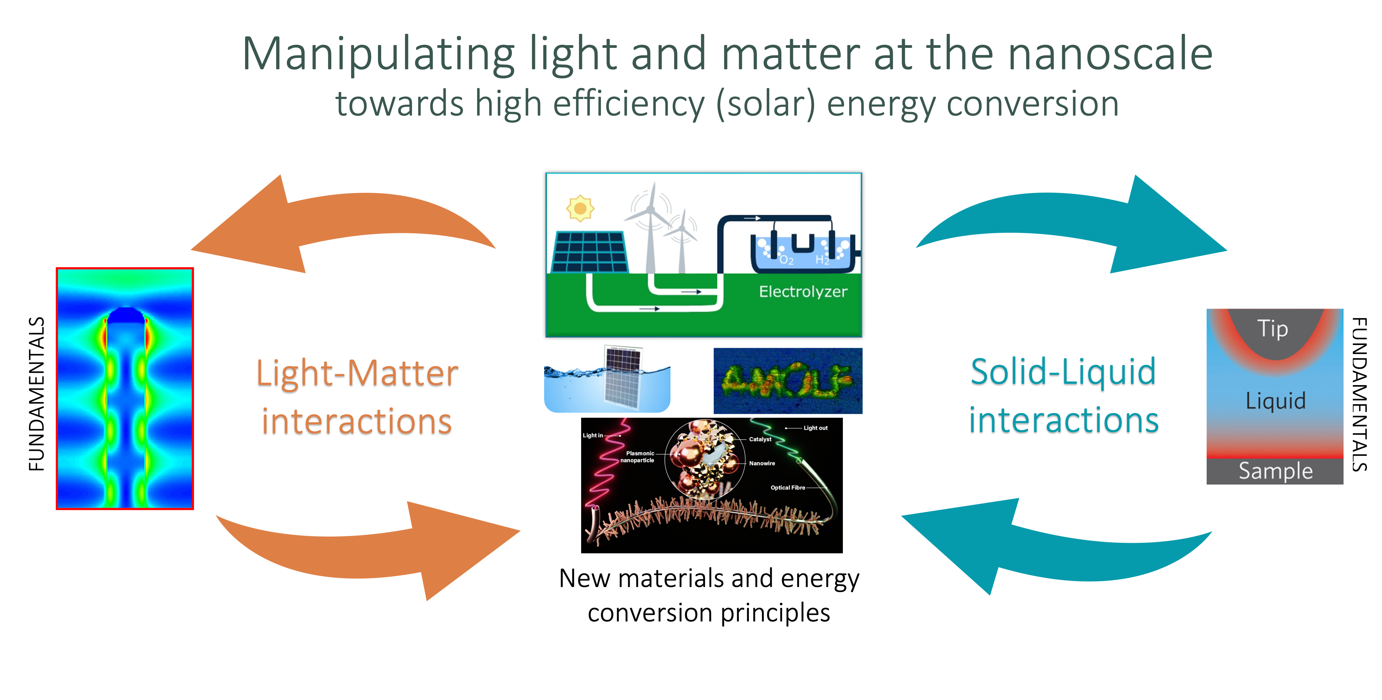
Our group focuses on the manipulation of light and matter at the nanoscale with nanophotonic and nanoelectrochemistry concepts, and viceversa. With this focus, our aim is to understand and gain full control over two key phenomena in solar energy conversion: light-matter interactions and charge transport at/through interphases. While there is plenty to explore in these two fields, we are also interested in the synergistic interplay between these two phenomena, enabling new types of light-controlled material growth, chemistry and electro-catalysis at the nanoscale. With the high level of control over where and how reactions take place, we seek to develop new energy conversion concepts with higher conversion efficiency with less quantity and more cost-effective materials.
More specifically, we focus on:
– Developing new earth-abundant material designs for more efficient, selective and cost-effective energy conversion, including solar to electrical, solar to chemical and electrical to chemical energy.
– Underpinning the key physico-chemical properties of solid-liquid interfaces that rule charge transfer and conversion from electrical to chemical energy
– Developing new in-situ measuring techniques with which electrochemical, optical and surface properties of materials can be determined with nanoscale resolution. These include in particular, the development of in-situ and operando scanning probes
– Developing new light-management strategies for low-cost thin film solar energy conversion devices, including solar cells and photoelectrochemical cells