Nanomaterials, nanofabrication
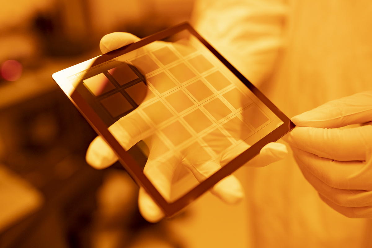
Direct electrochemical writing of metals and semiconductors
Group: 3D Photovoltaics
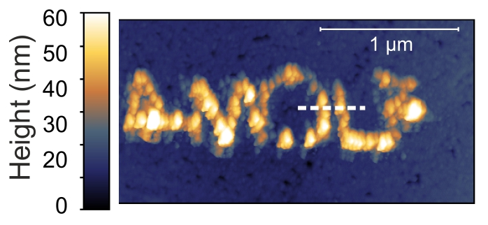
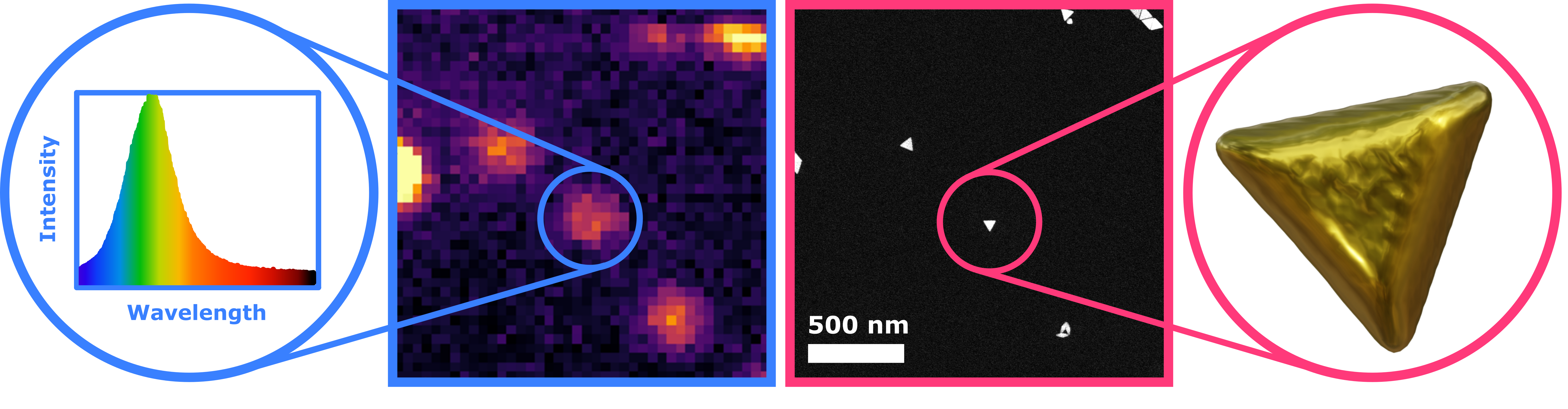
We use the tip of an electrochemical atomic force microscope to localize and direct the electrodeposition of materials at the nanoscale. This process is done in solution and driven electrically.
Potential applications
- Maskless/additive nanofabrication
- Markerless overlay
- Novel 3D structures
Reference
M. Aarts and E. Alarcón-Lladó, Directed nanoscale metal deposition by the local perturbation of charge screening at the solid–liquid interface, Nanoscale 11, 40: 18619-18627 (2019)
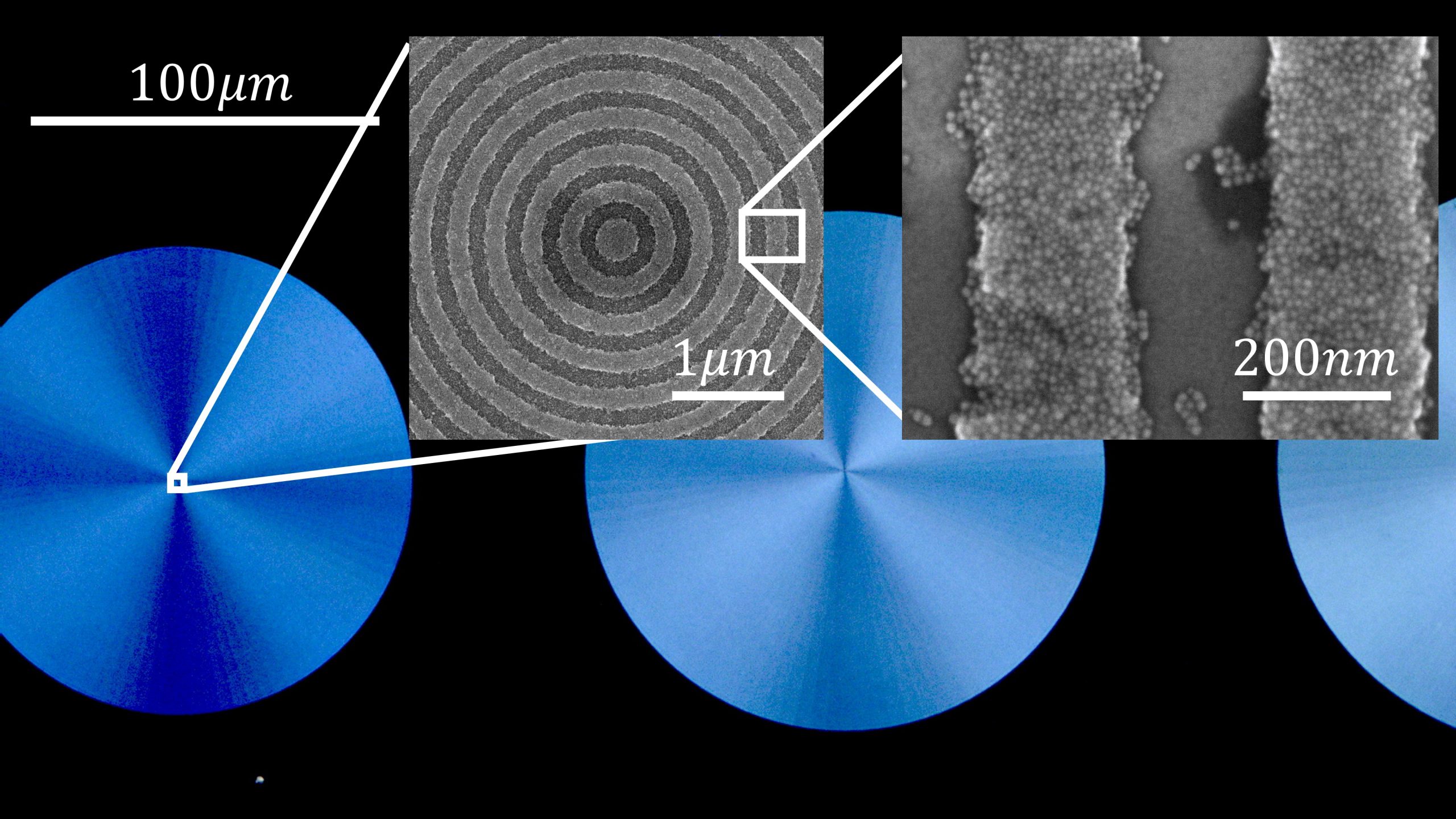
Nanofabrication of metasurfaces using electrodeposition/electroplating
Group: 3D Photovoltaics
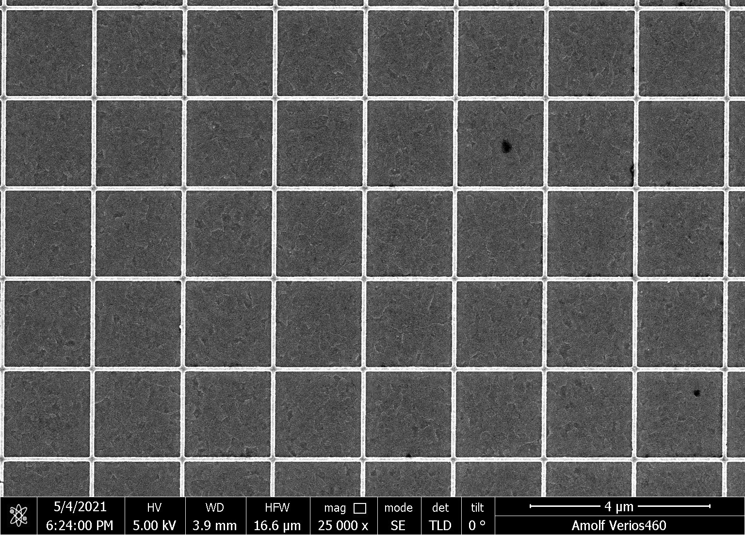
We develop a electrochemical method to fabricate pre-designed metallic nanostructures for the usages as transparent conducting electrodes. This method provides an opportunity to mass produce metallic nanostructures for solar cell devices.
Potential applications
- Light trapping in solar cells
- Ultra thin flexible solar cells
- Ultra transparant touchscreens
- Color selective displays
Nanopatterning of semiconductor quantum dots
Group: Hybrid Solar Cells
Semiconductor quantum dots are excellent light emitters, whose color of emission can be tuned by changing their size. Nanopatterning of these particles into larger structures provides an additional handle to change their light emission properties, e.g.directionality.
Potential applications
- Patterning of II-VI (PbS, CdSe) and perovskite quantum dots
- Patterning by e-beam or (E)UV lithography
- Structures remain luminescent, allowing for applications in light-emitting devices
Interaction between components in complex hybrid nanosystems such as metal-semiconductor structures
Group: Hybrid Nanosystems
We want to understand the interplay of properties and morphology by combining advanced (in situ) electron microscopy/tomography with single particle optical techniques. We are also interested in new concepts to create hybrid structures and the use of external stimuli to modify them.
Potential applications
- Solar harvesting (photovoltaics and photocatalysis)
- Information processing
Reference
W. Albrecht, E. Bladt, H. Vanrompay, J. D. Smith, S. E. Skrabalak and S. Bals, Thermal Stability of Gold/Palladium Octopods Studied in Situ in 3D: Understanding Design Rules for Thermally Stable Metal Nanoparticles, ACS Nano 13, 6522-6530