Solar cell wonder material surprises researchers : Unexpected experimental results lead to a better understanding of promising perovskite
Physicists at AMOLF have unraveled the mysterious working mechanism of a promising new class of materials for solar cells. Their pressure experiments with perovskite semiconductors had very counter-intuitive results, which could not be explained by the theory for conventional semiconductors. However, the results matched surprisingly well with a novel theory developed at Imperial College in London, predicting a peculiar band structure in perovskite materials. “Theory and experiments came together perfectly and helped us solve an important part of the perovskite puzzle”, says AMOLF group leader Bruno Ehrler, who published the results in Energy & Environmental Science on 23 December 2016.
A new material class based on lead-halide perovskite semiconductors is generating a lot of attention in the solar cell research community. Only five years after their incidental discovery, solar cells made from these perovskite materials reach efficiencies close to that of the best silicon solar cells. Furthermore, perovskites can be printed like ink, which makes cheap, large-scale production a realistic prospect. “Device progress is very fast, but at the same time we hardly understand why these materials perform so efficiently”, says Bruno Ehrler, head of the Hybrid Solar Cells group at AMOLF. “When light hits the active material of a solar cell, free electrons are generated, which can be extracted as electrical power. In perovskite materials, the free electrons live much longer than expected from a semiconductor with such a strong light absorption.”
Perovskite under pressure
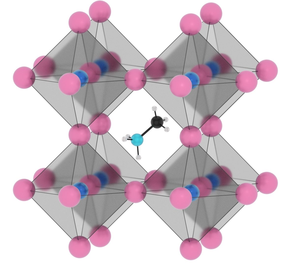
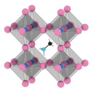
The long lifetime of free electrons in the perovskite allows plenty of time for extraction of electrical power in solar cells. Ehrler’s team was hit by surprise, however, when they applied high pressure to a perovskite semiconductor (methylammonium lead iodide perovskite). The researchers discovered that the free electrons decay much faster under pressure and they expected the emission of light to also be reduced. “But the contrary happened; we saw a doubling of the light emission”, says AMOLF PhD student Tianyi Wang. “This result just would not make sense in the traditional picture of a semiconductor, and we re-measured many times to confirm that it was not an experimental artefact. “
Peculiar band structures
The researchers turned to colleagues at Imperial College London, who in collaboration with King’s College London recently developed a novel theory to describe perovskite materials. This theory predicted a very unusual band structure which protects the electrons in perovskite semiconductors from decay. “Semiconductors can be classified into two distinct types, direct and indirect bandgap semiconductors”, Ehrler explains. “Direct bandgap semiconductors absorb light strongly, but the electrons also decay quickly. Indirect bandgap semiconductors, such as the widely used silicon, absorb light much more weakly, but the indirect bandgap protects the electrons from decay, leading to a much longer lifetime. According to the new theory, the perovskite material offers both, a direct and indirect bandgap, which have very similar energy level. This means that electrons experience both types of bandgap, leading to strong absorption and an unusually long lifetime.”
Theory confirmed
The theory of a dual bandgap structure for perovskite materials also predicts that under pressure, the protection of free electrons by the indirect bandgap fades, and the material behaves more like a conventional direct bandgap semiconductor. “With this theory in mind, our experimental data suddenly did make perfect sense,” says Benjamin Daiber from AMOLF. His colleague Aron Walsh from Imperial College was glad to see his prediction confirmed in the experiment: “Of course we strongly believe in the theoretical prediction, but without experimental evidence, it is much harder to convince the scientific community we solved part of the perovskite puzzle.”
Ehrler acknowledges that perovskite materials have not revealed all their mysteries yet. “The next step is to investigate which part of the perovskite crystal structure is responsible for the unusual band structures we found and discover what kind of bandgap would be best for solar cells and other applications”, he says. “Our results suggest that we can change the properties of perovskite semiconductors fundamentally. This may lead to more efficient light emitting diodes (LEDs) and lasers made from perovskite materials. It further creates opportunities to better control the development of completely new materials.
Reference
Tianyi Wang, Benjamin Daiber, Jarvist M. Frost, Sander A. Mann, Erik C. Garnett, Aron Walsh and Bruno Ehrler. Indirect to direct bandgap transition in methylammonium lead halide perovskite under pressure. Energy Environ. Sci., 2016, DOI: 10.1039/c6ee03474h