Painting with semiconductors

AMOLF researchers Lukas Helmbrecht and Wim Noorduin have developed a reactive ink that can be painted on an equally reactive canvas. The ink reacts with the material on the canvas to become a semiconductor that emits colored light, an essential part of electronic components such as LEDs. Consequently, a new way of producing these electronic components is now within reach. The results of the research, a collaboration between the AMOLF groups Self-Organizing Matter and Hybrid Solar Cells, are published this week in the journal ‘Advanced Materials’.
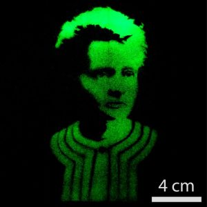
Imagine that you could paint a canvas by making the canvas itself change to a different color instead of brushing paint on it. That is what Lukas Helmbrecht and his colleagues are doing with the new ion exchange lithography technique. In this technique, the ‘ink’ reacts with the ‘canvas’ by means of ion exchange. Helmbrecht put his money where his mouth is and used this technique to airbrush an image of Madame Curie. “I find it fascinating to see: the green image forms as soon as you start spraying, despite both the ink and the canvas being colorless.”

Colorful technique
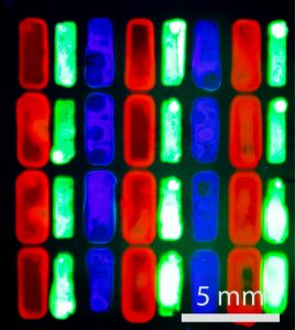
The research revolves around producing perovskite, a new and highly promising semiconductor material used to produce items such as LEDs and solar cells. Helmbrecht and his colleagues found a way of converting a layer of lead carbonate (the canvas) into a perovskite, simply by ‘painting’ on it with a solution of methylammonium bromide. The latter undergoes a chemical reaction with the lead carbonate to form a green-emitting perovskite. Using a solution of a different substance as the ink allows you to paint a blue- or red-emitting perovskite next to this, or to airbrush or print a pattern.
A wide range of variations in the composition of the perovskites is possible by choosing different inks. The patterns can be created very accurately: drops of ink just a few micrometers in size also yield dots just a few micrometers in size. This means the ink does not run. “The challenge of this research was developing the chemical reaction and the conditions: the quantity of ink, the pressure, and the properties of the canvas. None of these were known, and the process does not work if they are not exactly right,” says Helmbrecht.
Everything in a single layer
The comparison with other techniques for applying layers of perovskites to a carrier springs to mind. But this technique is fundamentally different, Helmbrecht explains. “All traditional techniques result in different layers of perovskite next to each other or on top of each other. Our method results in a single layer that consists of different types of perovskite.” In addition, perovskites are usually quite sensitive to the treatments used in traditional methods, such as etching or rinsing. These can damage the perovskite. With ion exchange lithography, these treatments are no longer needed.
“In principle, this is a far simpler method for applying a pattern of different perovskite semiconductors next to each other on a chip or LED,” Helmbrecht says. Cleanrooms or other special conditions are no longer required. The researchers have demonstrated the utility of ion exchange lithography by using the technique to produce a working LED. “That has proven the principle.” Different groups within AMOLF will start using this technique to create other applications.

Reference
L. Helmbrecht, M.H. Futscher, L.A. Muscarella, B. Ehrler, W.L. Noorduin, Ion Exchange Lithography: Localized Ion Exchange Reactions for Spatial Patterning of Perovskite Semiconductors and Insulators, Advanced Materials (2021).


