
Nanoscale optical tomography using electrons
A team of researchers from AMOLF and Stanford University has developed a novel way to make three-dimensional optical images of nanoscale objects. They irradiate the object with a 30 keV electron beam under different angles and collect the cathodoluminescence emitted by the sample. Using a tomographic reconstruction they then determine the three-dimensional light distribution in metallic crescent particles at nanoscale resolution.
Cathodoluminescence
Many novel optical devices, such as solar cells, LEDs or lasers require control over the concentration of light at the nanoscale. However, standard optical microscopy cannot be used to probe light at this scale as the imaging resolution is limited by the optical diffraction limit (~250 nanometer). A new instrument, developed in Albert Polman’s group at AMOLF in the past years, uses an electron beam to excite materials and detects the emitted light (called cathodoluminescence) to make optical images at a resolution far below the diffraction limit. So far, however, only two-dimensional images were made.
Tomography
The new study, published in Nature Nanotechnology on April 6th, 2015, expands this technique to carry out three-dimensional tomography. Combining expertise from the groups at AMOLF and Stanford, the team uses 30 keV electrons to excite crescent-shaped core-shell particles composed of a polystyrene core and a gold shell. These particles, with a diameter of 250 nanometer, serve as a model system in which multicolored light is concentrated in different nanoscale focal spots. The research team irradiated crescents with electrons under multiple angles, collected the emitted light and carried out a tomographic reconstruction. In this way multicolored optical hot spots were imaged in three dimensions at a resolution smaller than the diffraction limit.
The Stanford part of the team was led by Jennifer Dionne, an assistant professor in Stanford’s Department of Materials Science and Engineering. Dionne is a long-term collaborator of AMOLF in the field of plasmonics and optical metamaterials. Dionne and Polman: “This was an exceptional project that became successful because of the complementary expertise of all of us. Together we are exploring new application areas that are opening up. We are already applying the images in the characterization of solar cells. We also think our new technique could be modified for imaging biological systems without the need for fluorescent labels.”
Reference
A. Atre, B.J.M. Brenny, T. Coenen, A. Polman and J.A. Dionne, Nanoscale optical tomography with cathodoluminescence spectroscopy Nature Nanotech. 10, 429–436 (2015) | DOI: 10.1038/nnano.2015.39
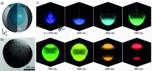
3D tomograms of nanoscale light (a) Schematic of crescent particle composed of a polystyrene core and Au shell. (b) Transmission electron micrograph of a crescent particle, showing a sharp Au edge revealing the bare polystyrene core at the top-right corner. (c) Cathodoluminescence tomograms at different wavelengths. A blue optical hot spot is observed at the bottom center inside the particle while a red hotspot is observed within the cusp at the top.

© AMOLF/Stanford/Tremani