A crucial step towards better performing solar cells
Solar cells need monocrystalline materials to work optimally. But the traditional way to build monocrystalline materials is highly time consuming. AMOLF physicists in the Nanoscale Solar Cells group have found a new way of building them, which is at least a hundred times more efficient. This research has been published in the journal Advanced Materials on 3 May 2017.
Rock candy
In monocrystalline materials, all atoms are perfectly ordered, which makes them highly conductive. That is why they are used to optimise the performance of optoelectronic devices like solar cells.
Traditionally, crystals are made from a ‘seed’. This follows the same principle as creating rock candy: when a stick is immersed into a supersaturated solution of water and sugar, a sugar crystal will start to form on the stick. On this seed, a bigger crystal can be grown.
The problem is that when a crystal is growing from one seed, it is very hard to control the ultimate structure of the crystal and therefore it will end up bulky. Consequently, a lot of steps are needed to cut the crystal down to a small scale to make a transistor for example, which is extremely small and thin.
Tiny cubes
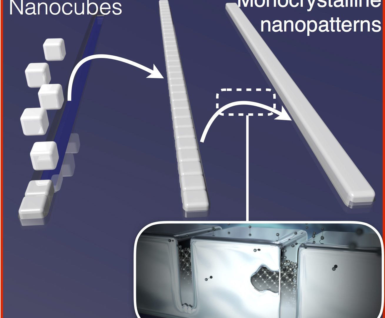
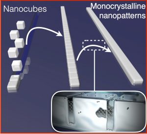
AMOLF physicists have found a way to maintain control over the structure of the crystal from the beginning. This allows them to build monocrystalline materials in a much more efficient way. “Our approach is different from the traditional method, because we are using billions of seeds to grow our crystals,” says group leader Erik Garnett.
In this method, the seeds are tiny cubes that can be stacked together to make larger crystals with a programmable 3D shape. A rubber stamp with little cube-sized canals is used to stack the tiny cubes together in the preferred pattern. After that, the cubes are glued together.
Glue
Garnett and his team are the first to find a way to glue the tiny cubes together. “Although the gaps between the cubes might be only a few atoms wide, it is crucial to glue them together in order for the cubes to act like one big crystal,” Garnett explains. During the gluing process, single atoms fill in the gaps between the cubes like bridges, which is called chemical welding.
Advantages
This new way of building monocrystalline materials has several advantages over the old method, says Garnett. “First, it is at least a hundred times more efficient, because we can build crystals in the desired shape from the beginning. This prevents us from having to cut a bulky piece of crystal in the right shape following a lot of time-consuming steps. Second, our method uses low temperatures, which is easier, cheaper and better for the environment. Third, our method could be used to build crystals of materials not compatible with the standard process.”
Silver
For this first proof-of-concept, Garnett and his team used silver to build the monocrystalline material. Silver is also used in solar cells, but until now only in polycrystalline form. In polycrystalline materials, the atoms are not aligned in the same way, and are therefore far less conductive. “Our research is the first to show a practical way to make monocrystalline silver. Because of the higher conductivity, lower amounts will be needed. This will not only save money, but is also important to avoid a future shortage of silver.”
Future
Applying this process for monocrystalline materials to copper rather than silver has even greater application potential. Copper is cheaper and as conductive as silver and already used extensively in computer chips. Therefore, Garnett and his team are now working in this direction. Furthermore, they are working on scaling up the process: “We are also investigating a way to make monocrystalline materials over a larger area. We are already able to make crystals at the microscale, which can be used for transistors. Now we want to be able to make crystals for solar cells, which need to be at a centimetre scale.”
Reference
Sciacca, A. Berkhout, B.J.M. Brenny, S.Z. Oener, M.A. van Huis, A. Polman and E.C. Garnett, Monocrystalline Nanopatterns Made by Nanocube Assembly and Epitaxy, Adv. Mater. advanced article, (2017)