
A low-tech way to create high-tech materials
AMOLF researcher Christiaan Van Campenhout has found a new, simple method to create a material with a regular pattern of crystalline bands. The pattern formed by the crystals is not a coincidence. With a simple setup, the researchers can precisely control the width of the bands and their spacing. This could be a straightforward and cost-effective way to produce optics, electronics, or sensors. The research was published in the journal Advanced Materials on August 2, 2023.
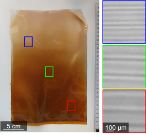
In all its simplicity, the experiment and its results are remarkable. The plastic sheet appears rather ordinary with its brownish color. However, when a laser beam passes through it, a pattern of dots emerges on the other side: the result of the regular narrow bands of crystals embedded in the plastic, invisible to the naked eye. Typically, such precise control over pattern formation for electronics requires expensive and complex techniques like lithography. Van Campenhout conducts his research in the Self-organizing matter group led by Wim Noorduin, in collaboration with the Mechanical Materials group led by Martin van Hecke. The goal is to discover simple, nature-inspired methods to create such components. “In nature, you find regular patterns everywhere, from the stripes of a zebra to the patterns on a butterfly wing. We want to use a self-organizing, biologically inspired strategy to create high-tech materials. This research is a good step in that direction.”
Dipping instead of shrinking
The crystals in the pattern form through a chemical reaction between a substance in a gel (which solidifies into a plastic sheet after the experiment) and a substance in a solution that diffuses into the gel. The formation of crystal bands in this so-called reaction-diffusion process was already known. Last year, the researchers published an article demonstrating that they could create a regular band structure by slightly shrinking the gel. This observation got them thinking: can it not be simpler than shrinking? “We noticed that the liquid level and the location of the reaction in the gel remained at an equal distance from each other during the shrinkage. This leads to the regular band structure. We thought that we might achieve the same result by gradually dipping the gel into the liquid instead of letting the liquid diffuse into the gel”, explains Van Campenhout. This straightforward setup worked right away, much to Van Campenhout’s delight: “This is my favorite kind of research: not overanalyzing but thinking: can’t it be simpler? And then it works.” The process was named R-DIP: reaction-diffusion driven immersion-controlled patterning.
Smaller bands for applications
It quickly became evident that the distance between the bands depends on the speed at which the liquid level rises. The faster you dip the gel into the liquid, the closer the bands will be to each other. Initially, the distance between the bands was 200 micrometers (0.2 mm) with a variation of only 6 micrometers. Currently, the smallest band distance is 7 micrometers. “For many interesting applications, it’s essential to have the bands even closer together, around 0.2 micrometers or less”, says Van Campenhout. The research will focus on achieving that goal in the coming period. Van Campenhout also demonstrated that the method is scalable: it works with a sheet the size of an A4 paper. “This suggests that it’s suitable for roll-to-roll production, a method already used for large-scale electronics manufacturing.” Additionally, you can overlay several sheets with bands, each one slightly rotated. “This allows us to create a polarizing film for items like sunglasses and lenses.” Another application is an ultra-sensitive pressure sensor. When you place two layers parallel to each other, they create a so-called Moiré pattern, which changes as the layers are slightly pressed together. “You can observe a visible change with the naked eye when the gel is pressed for 20 micrometer”, explains Van Campenhout. In the coming period, Van Campenhout will investigate whether he can change the composition of the bands through chemical modifications to make them more suitable for applications. This could possibly be achieved using methods previously developed by Noorduin’s group to convert calcium carbonate into semiconductors. Moreover, the films resemble photographic film, in which silver salts also contribute to color and contrast. “We are investigating whether we can apply the chemical knowledge from photography to develop films for other applications.”
Reference
Christiaan T. van Campenhout, Hinco Schoenmaker, Martin van Hecke, Willem L. Noorduin, Patterning complex line motifs in thin films using immersion controlled reaction-diffusion. Advanced Materials, August 2 (2023).
https://doi.org/10.1002/adma.202305191