Nano-tetris for Monocrystallinity
In this project we assemble nanocubes by the virtue of capillary forces on a flexible stamp. Subsequently, the assembled cubes can be printed onto a variety of substrates like Si, TEM grids, glass etc. Eventually the cubes are welded together to form a single crystal. The pattern of the crystal/thin film is governed by the design of traps for cubes on the template. The methodology combines best of both worlds meaning benefits of top-down (patterning) as well as bottom-up (efficient material utilization) nanofabrication and key feature being that it enables fabrication of patterned thin films of metals. This novel approach fundamentally uses epitaxy between adjacent cubes and eliminates the substrate dependence for overgrowth. Thus, it can be potentially extended to all classes of materials.
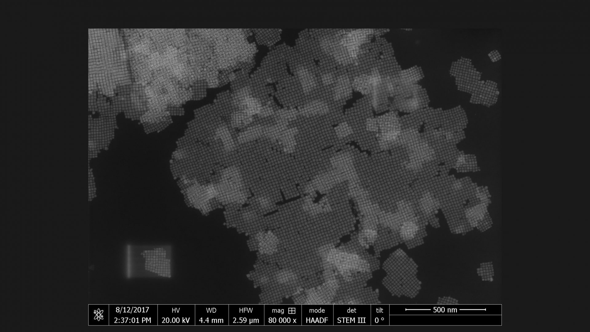
We have demonstrated this process for metals like Ag and Pd and semiconductors like CsPbBr3. We are also interested in taking it one step further and study the quality of welded interface by 3D electron tomography which will enable us to study local stress distribution, formation of dislocations as well as other defects, if any.
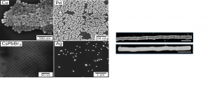
Picture (left): Variety of nanocubes synthesized in our lab. Picture (right): Upper panel depicts the assembly of 70 nm Ag cubes and the lower panel depicts the welded single crystal of the same.
Reference
Sciacca et. al., Monocrystalline Nanopatterns Made by Nanocube Assembly and Epitaxy, Adv. Mater. 2017, 29, 1701064.
Brainpower: Biblab Patra and Harshal Agrawal