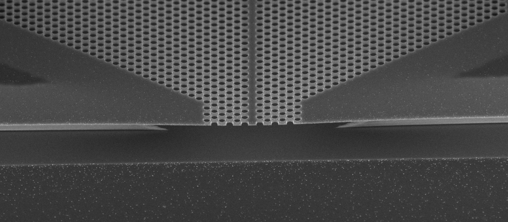
Raith e-LiNE lithography system
With an electron beam a pattern is written in a photoresist layer. After exposure to this beam it is possible to selectively remove either exposed or non-exposed regions of the resist with chemicals thus creating nanotechnology structures.

Specifications
- Sample loadlock
- Universal sample holder for small sample pieces up to 100mm 10mm max height
- Electron beam energy 10 – 50kV
- Beam current range 50 pA – 40 nA
- Beam size < 2.5 nm diameter at 50 kV
- Beam current stability <0.5% / h
- Beam position stability < 200 nm / 8h
- Patterning area 150mm by 150mm symmetrical
- Pattern generator 50 MHz pixel frequency
- 20 ns minimum dwell time
- Stage range x=150 by y=150mm z=20 mm
- Laser-interferometer X –Y stage with 1 nm position resolution
- Z – axis Laser Height sensing reproducibility 1 micron
- Write field stitching 35 nm in 500 micron write field
- Minimum feature size 20 nm in high resolution positive resist
- Mark recognition gives overlay accuracy of 35 nm
- GDSII format viewer and editor
- Import AutoCAD DXF,bitmap, ASCII or CIF format converted to GDSII
- Traxx and Periodixx software option
- FBMS and MBMS software option