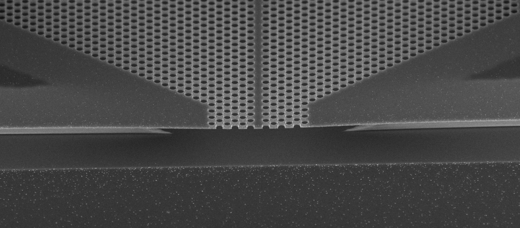
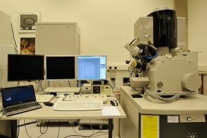
FEI Helios Nanolab 600
This SEM / FIB combines a scanning microscope (SEM) and gallium focused ion beam (FIB) with gas chemistries.
Specifications
- FEI Helios Nanolab 600
- Sample size max. diameter 150 mm thickness 20 mm
- SEM; Schottky Field Electron Gun (SFEG)
- Electron beam; 1pA to 22 nA, 350V- 30kV, 1 nm resolution
- FIB: Sidewinder Galium Liquid Metal Ion Source (Ga LMIS)
- Galium Ion beam; 1.5pA – 20 nA, 500V- 30kV, 5 nm resolution
- Charge neutralizer
- 5 axis UHR motorized sample stage; XY: 150mm, Z: 10mm, Tilt: -10° to +60°, rotation: 360° endless
- NavCam sample navigation
- detectors;
-ETD (Everhardt Thornley Detector)
-TLD (Through the Lens Detector)
-CDEM for secondary electron and secondary ion imaging
-IR camera for sample navigation - Gas injector system (GIS);
-Platinum metal deposition
-SiO2 Insulator deposition (TEOS)
-Carbon deposition
-Insulator enhanced etch (XeF2) - Fast Beam Blanker
- Sample load lock
- Plasma cleaner (Evactron)
- Cryo Cleaner